SKIN CANCER DETECTION USING ABCD RULE
Abstract:
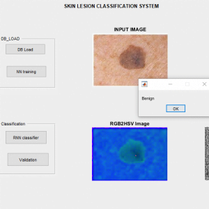
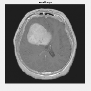
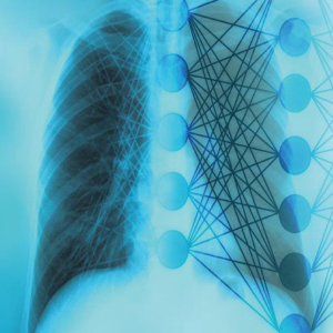
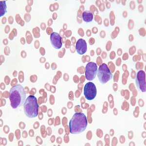
Human Cancer is one of the most dangerous diseases which is mainly caused by genetic instability of multiple molecular alterations. Among many forms of human cancer, skin cancer is the most common one. To identify skin cancer at an early stage we will study and analyze them through various techniques named as segmentation and feature extraction. Here, we focus malignant melanoma skin cancer, (due to the high concentration of Melanoma- Hier we offer our skin, in the dermis layer of the skin) detection. In this, we used our ABCD rule dermoscopy technology for malignant melanoma skin cancer detection. In this system different step for melanoma skin lesion characterization i.e, first the Image Acquisition Technique, pre-processing, segmentation, define feature for skin Feature Selection determines lesion characterization, classification methods. In the Feature extraction by digital image processing method includes, symmetry detection, Border Detection, color, and diameter detection and also we used LBP for extract the texture based features. Here we proposed the Back Propagation Neural Network to classify the benign or malignant stage.
Introduction
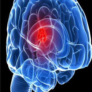
Skin cancers are cancers that arise from the skin. They are due to the development of abnormal cells that have the ability to invade or spread to other parts of the body.
There are three main types of skin cancers: basal-cell skin cancer (BCC), squamous cell skin cancer (SCC) and melanoma. The first two, along with a number of less common skin cancers, are known as non melanoma skin cancer (NMSC).
Basal-cell cancer grows slowly and can damage the tissue around it but is unlikely to spread to distant areas or result in death. It often appears as a painless raised area of skin that may be shiny with small blood vessel running over it or may present as a raised area with an ulcer.
Squamous-cell skin cancer is more likely to spread. It usually presents as a hard lump with a scaly top but may also form an ulcer. Melanomas are the most aggressive.
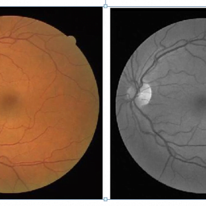
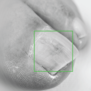
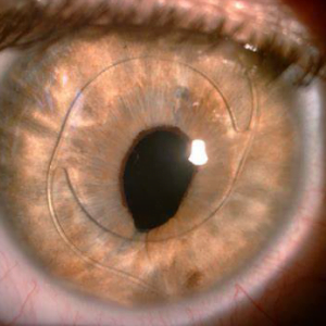
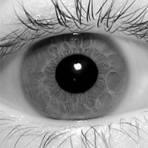
Signs include a mole that has changed in size, shape, color, has irregular edges, has more than one color, is itchy or bleeds.. A skin that has inadequate melanin is exposed to the risk of sunburn as well as harmful ultraviolet rays from the sun .Clinical analysis and biopsy tests are commonly used.
Existing Systems
- Principal Component Analysis
- Local binary pattern and shape features
- KNN and FNN classifier
Draw backs of Existing method
- High Computational load and poor discriminatory power.
- LBP doesn’t differentiate the local texture region.
- FNN is slow training for large feature set.
- Less accuracy in classification
Proposed Method
- Hybrid features involves colour features and texture descriptors
- ANN-Back Propagation Neural Network classifier
Advantages
- Fast and better compatible in classification.
- Low computational complexity
- Better efficiency and less sensitive to noise
- High accuracy
- Take less time for process
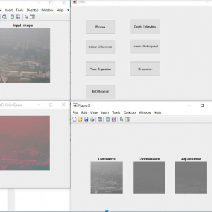
Block Diagram
Block Diagram Explanation
Colour Space Conversion
Color space conversion is happens when a Color Management Module (CMM) translates color from one device’s space to another. Conversion may require approximations in order to preserve the image’s most important color qualities.
The use of color in image processing is prompted with the useful resource of number one factors. First, shade is a powerful descriptor that frequently simplifies object identity and extraction from a scene. Second, human beings can determine plenty of shade solar shades and intensities, in comparison to approximately only two dozen sun sunglasses of gray. This 2d aspect is especially important in manual photo assessment
GLCM feature extraction
In statistical texture analysis, texture features are computed from the statistical distribution of observed combinations of intensities at specified positions relative to each other in the image. According to the number of intensity points (pixels) in each combination, statistics are classified into first-order, second order and higher-order statistics.
The Gray Level Co ocurrence Matrix (GLCM) method is a way of extracting second order statistical texture features. The approach has been used in a number of applications, Third and higher order textures consider the relationships among three or more pixels.
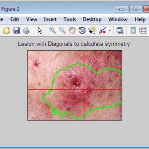
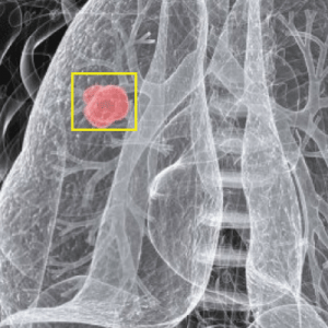
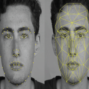
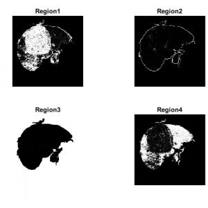
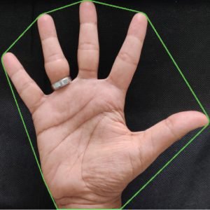
ABCD Parameters
The ABCDE Rule of skin cancer is an easy-to-remember system for determining whether a mole or growth may be cancerous. They describe the physical condition and/or progression of any skin abnormality that would suggest the development of a malignancy.
- A for Asymmetry
- B for Border
- C for Color
- D for Diameter
- E for Elevation
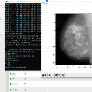
BPN Training and Classification
As is clear from the diagram, the working of BPN is in two phases. One phase sends the signal from the input layer to the output layer, and the other phase back propagates the error from the output layer to the input layer. For training, BPN will use binary sigmoid activation function Back-propagation is the essence of neural net training. It is the method of fine-tuning the weights of a neural net based on the error rate obtained in the previous epoch (i.e., iteration). Proper tuning of the weights allows you to reduce error rates and to make the model reliable by increasing its generalization
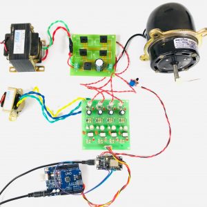
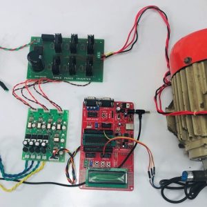
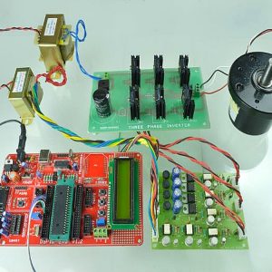
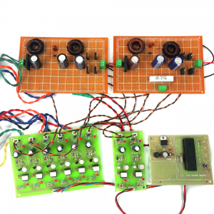
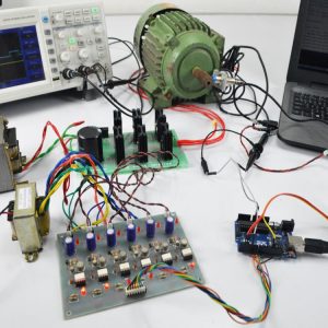
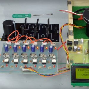
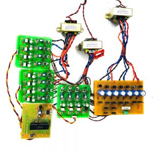
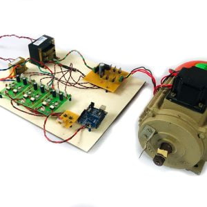
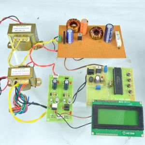
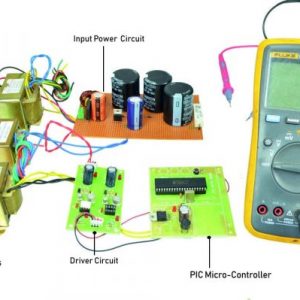
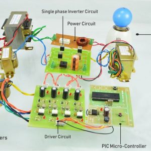
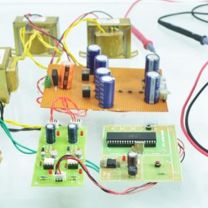
Requirement Specifications
Hardware Requirements
- system
- 4 GB of RAM
- 500 GB of Hard disk
SOFTWARE REQUIREMENTS:
REFERENCES
[1]Adheena Santy and Adheena Santy,Segmentation Methods For Computer Aided Melanoma Detection,IEEE Conference,2015.
[2] Omar Abuzaghleh, Miad Faezipour and Buket D.Barkana ,A Comparison of Feature Sets for an utomated Skin Lesion Analysis System for Melanoma Early Detection and Prevention,IEEE journal,2015.
[3] M. Rademaker and A. Oakley,Digital monitoring by whole body photography and sequential digital dermoscopy detects thinner melanomas,IEEE journal,2010.
[4] Xiaojing Yuan, Zhenyu Yang, George Zouridakis, and Nizar Mullani >
[5] Abder-Rahman Ali, Micael S. Couceiro, and Aboul Ella Hassenian ,Melanoma Detection Using Fuzzy CMeans Clustering Coupled With Mathematical Morphology,IEEE Conference,2014


Customer Reviews
There are no reviews yet.