


Description
Quadratic Boost Converter
ABSTRACT:
A Quadratic Boost Converter topology based on a high conversion ratio dc to dc converter with an active zero-voltage switching (ZVS) snubber circuit is developed for PV system application. The snubber circuit is used to protect the device and also provide smooth switching. The re-boost inductor, a coupled inductor, and charge-pump circuits are proposed to achieve the high voltage gain with a quadratic function. A first inductor is proposed to re-boost the voltage gain to make the output voltage is higher. The converter operating principle of the proposed conversion system is described in the detailed converter analysis. Simulation and experimental results are used to verify the performance of the quadratic boost converter with the maximum power point tracking controller (MPPT) in the PV inverter system.
EXISTING SYSTEM:
DC-DC converters are considered to be of great economic importance today and are widely used at home solar systems to produce the desired output power. DC Nano grid is a low-power dc distribution system suitable for residential power applications. The average load demand in the Nano grid is generally met by the local Renewable energy sources like solar, wind, etc. An energy storage unit is also required in the Nano grid to ensure an uninterruptible power supply to the critical loads and to maintain a power balance in the system. Fig.1 shows the general architecture of a nano-grid, consisting of both ac and dc loads. The diode D in the figure is associated as a series blocking diode in order to avoid reverse power flow. As the dynamic behaviors of all the different units of nano-grid are not uniform, they are interfaced to a common dc bus using power electronic converters, a solar panel as an energy source, a storage unit, and some dc and local ac loads. It incorporates three different power converter stages to interface with the renewable energy resources for ac as well as dc load.
PROPOSED SYSTEM:
In PWM (square-wave) dc-to-dc converter topologies, dc conversion ratio M is a function of duty ratio D of the active (transistor) switch. Both minimum and maximum attainable conversion ratios are limited in practical converters. Max is limited by the degradation in efficiency as duty ratio D approaches 1. On the lower end, minimum ON-time of the transistor switch results in a minimum attainable duty ratio and, consequently, in a minimum conversion ratio Min. The conversion range can be extended significantly if conversion ratio M has a quadratic dependence on duty-cycle. A quadratic boost converter (QBC) is a modified step-up converter with a single switch and a better conversion ratio.
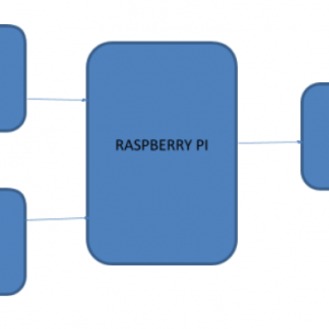
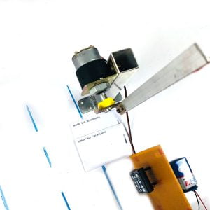
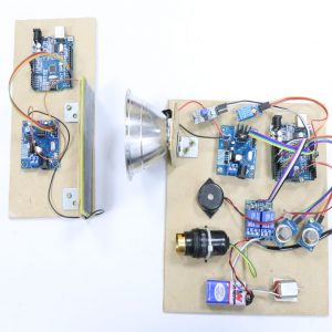
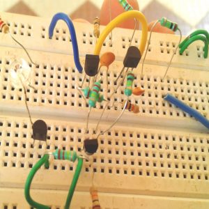
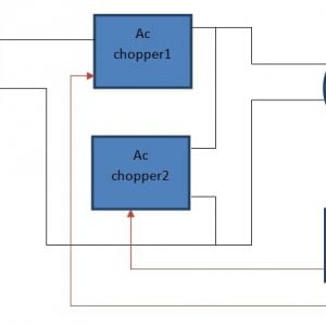
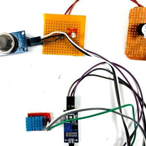
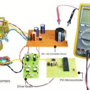
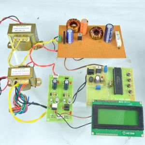
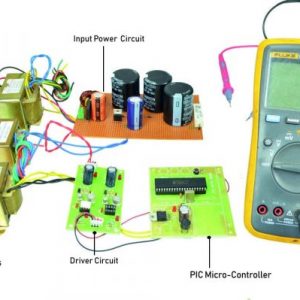
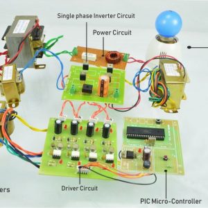
BLOCK DIAGRAM:


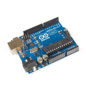
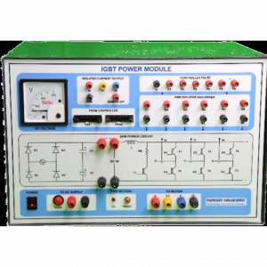
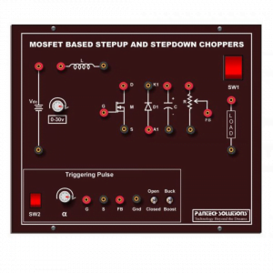
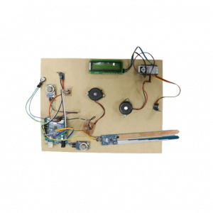
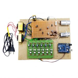
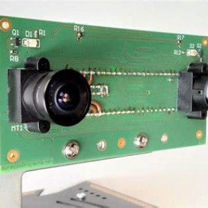
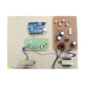
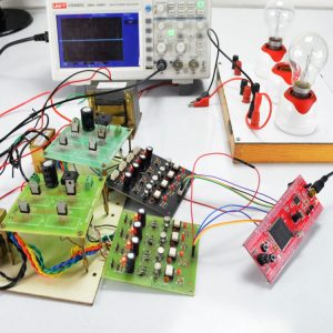
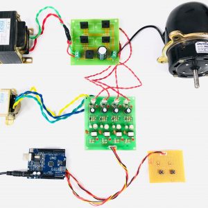
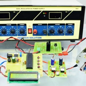
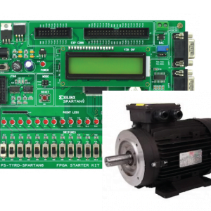
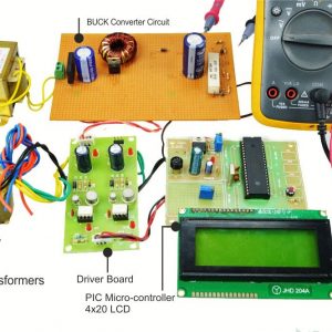
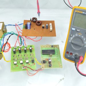
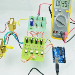
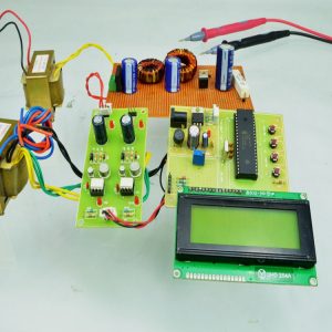
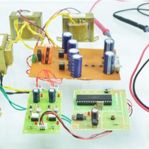
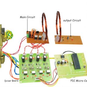
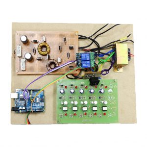
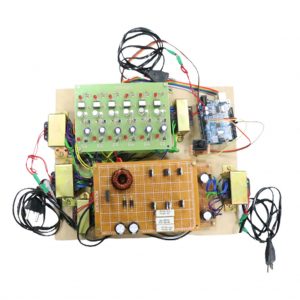
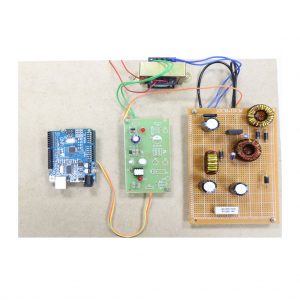
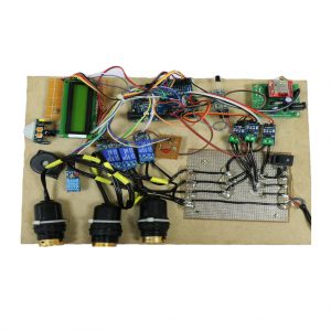
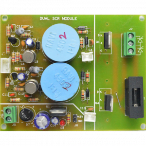
HARDWARE & SOFTWARE REQUIREMENTS:
HARDWARE
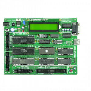
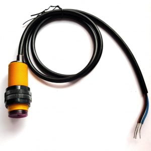
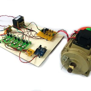
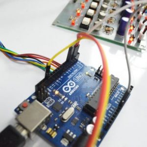
- PIC microcontroller(PIC16F877A)

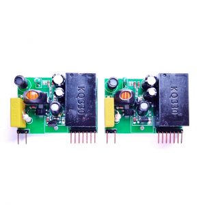
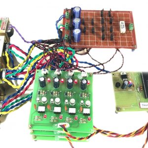
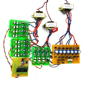
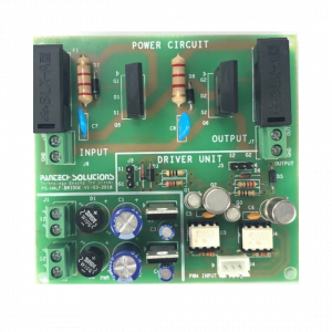
Quadratic Boost Converter 4 - Driver Board

SOFTWARE
- Matlab/Simulink
ADVANTAGES
- High efficiency
- Low cost
APPLICATIONS
- High gain dc voltages
- It suitable for high voltage conversions
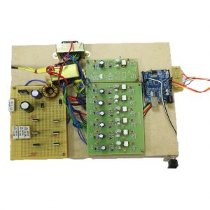
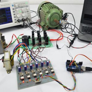
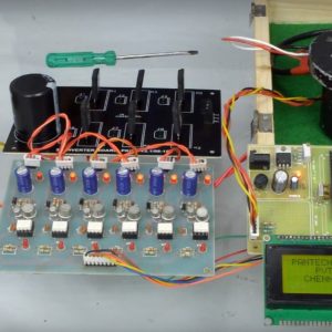
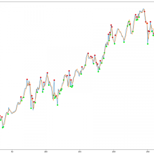
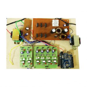
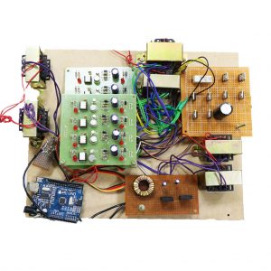
RESULT

CONCLUSIONS:
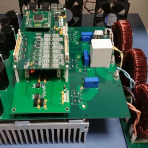
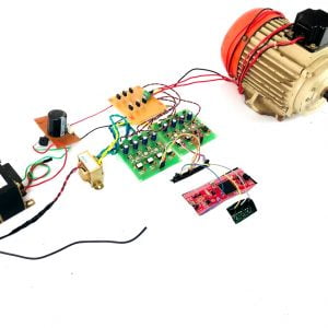
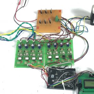
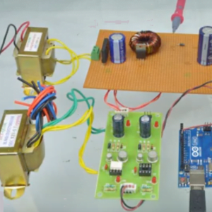
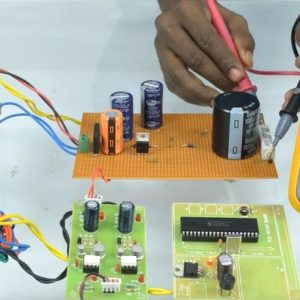
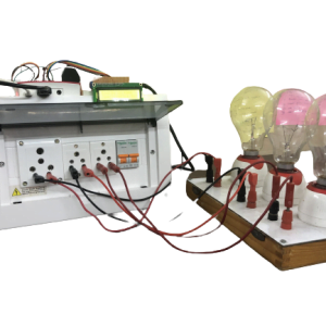
Compared to basic converter methods, the quadratic boost converter is a quadratic conversion ratio that offers a significantly wider conversion range. As far as conversion efficiency is concerned, it is quite clear that a single-stage converter is always a better choice than a two-stage converter. Therefore, the quadratic converters are proposed and intended for applications where conventional, single-stage converters are inadequate. The designed QBC circuit is simulated by MATLAB Simulink model and the results were verified by successfully building a 50W laboratory prototype.


Customer Reviews
There are no reviews yet.