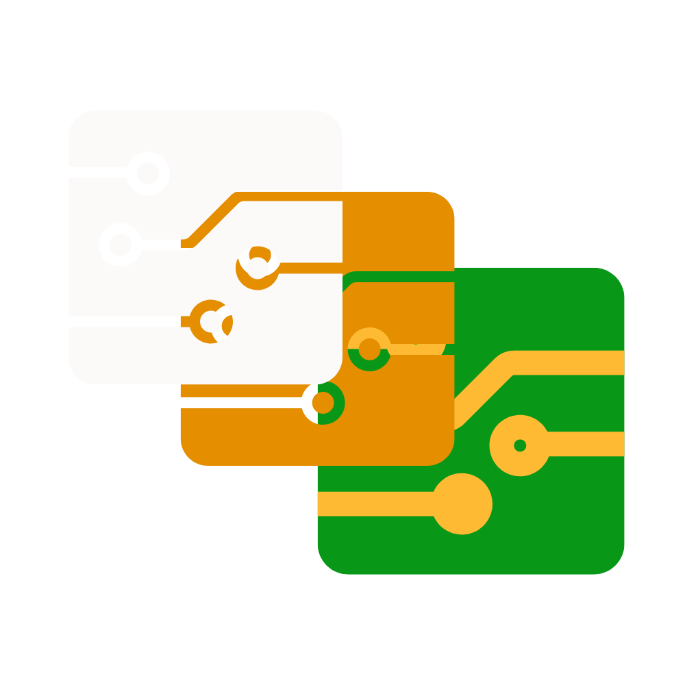
Enhance your PCB Design Skills and gain practical experience by taking part in this internship program that offers guidance from experienced professionals and access to industry-standard tools. Learn and apply to design single and multi-layer PCB’s as per Industry Standards
Explore the boundless possibilities of PCB Designing to the maximum potential.
This internship is designed to provide you with a comprehensive understanding of the Design aspects of PCB Design from scratch. By participating in this program, you will have the opportunity to gain hands-on experience with the tools and techniques that are being used by industry experts.
6+ Core PCB Concepts
Learn and Practice Schematic | Footprint | Single Layer | Double Layer | Cadance
15+ LIVE Projects
Implement Learned skills to develop LIVE Projects with Codes and Assistance
Program Highlights
Live / Recorded
Gain access to 30+ Records of High Value Content and Instructor Led Weekend LIVE Sessions
Community Supported
Become a Member of a Community of Highly Interactive Members and access to resources and Q & A Sessions
1 / 2 Months
Updated access to Records for 1 / 2 Months - Learn Anytime , Anywhere
Download PPT & Project Materials
Download Presentations and Project codes to practice while learning and implementation. Lifetime Access
How this Internship Program Works ?
Step 1 Enroll to the Program
✓ Gain Access to 30 Days of Record ✓ Get a Mentor Assigned
✓ Download Presentations & Practice Codes
✓ Learn at your Flexible Time
✓ Apprehend the concepts
Step 2 Attend LIVE Bootcamps
✓ Join the Private Community of Developers
✓ Attend LIVE Q & A Sessions
✓ Interact with the Mentor
✓ Practice the concepts
Step 3 Project Development
✓ Implement Skills Learnt
✓ Develop Projects with assistance
✓ Download Codes for Reference
✓ Implement Real-Time Data
✓ Visualise the Concepts
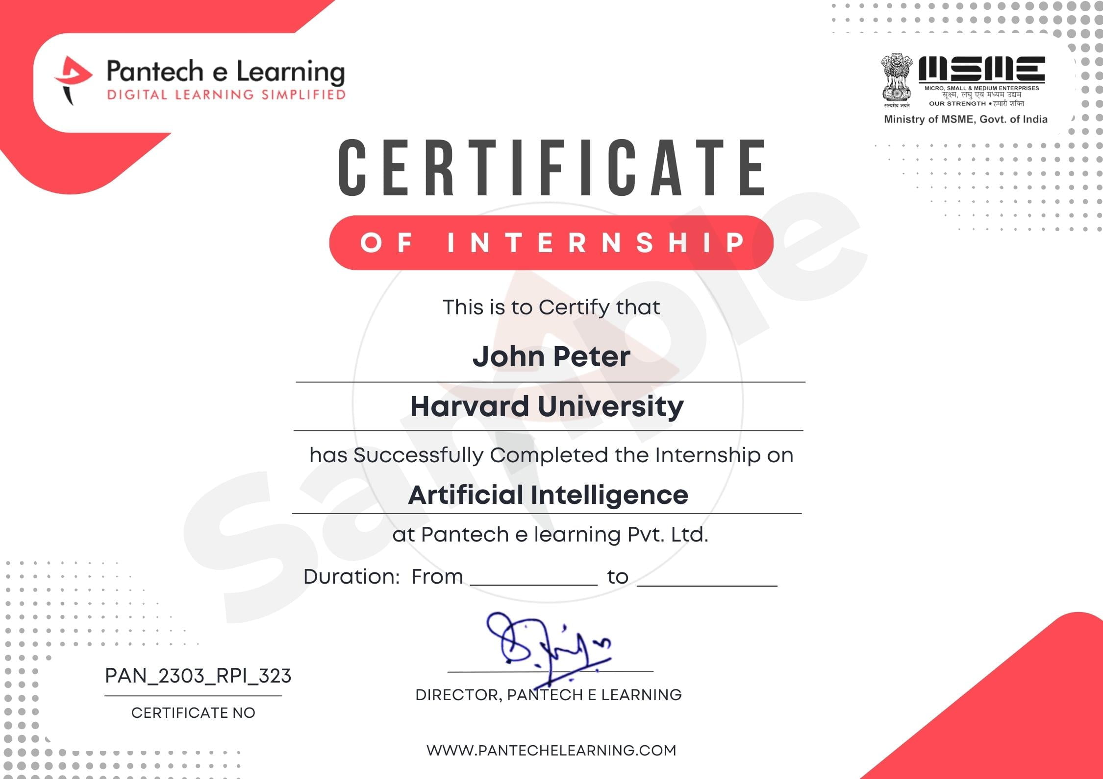
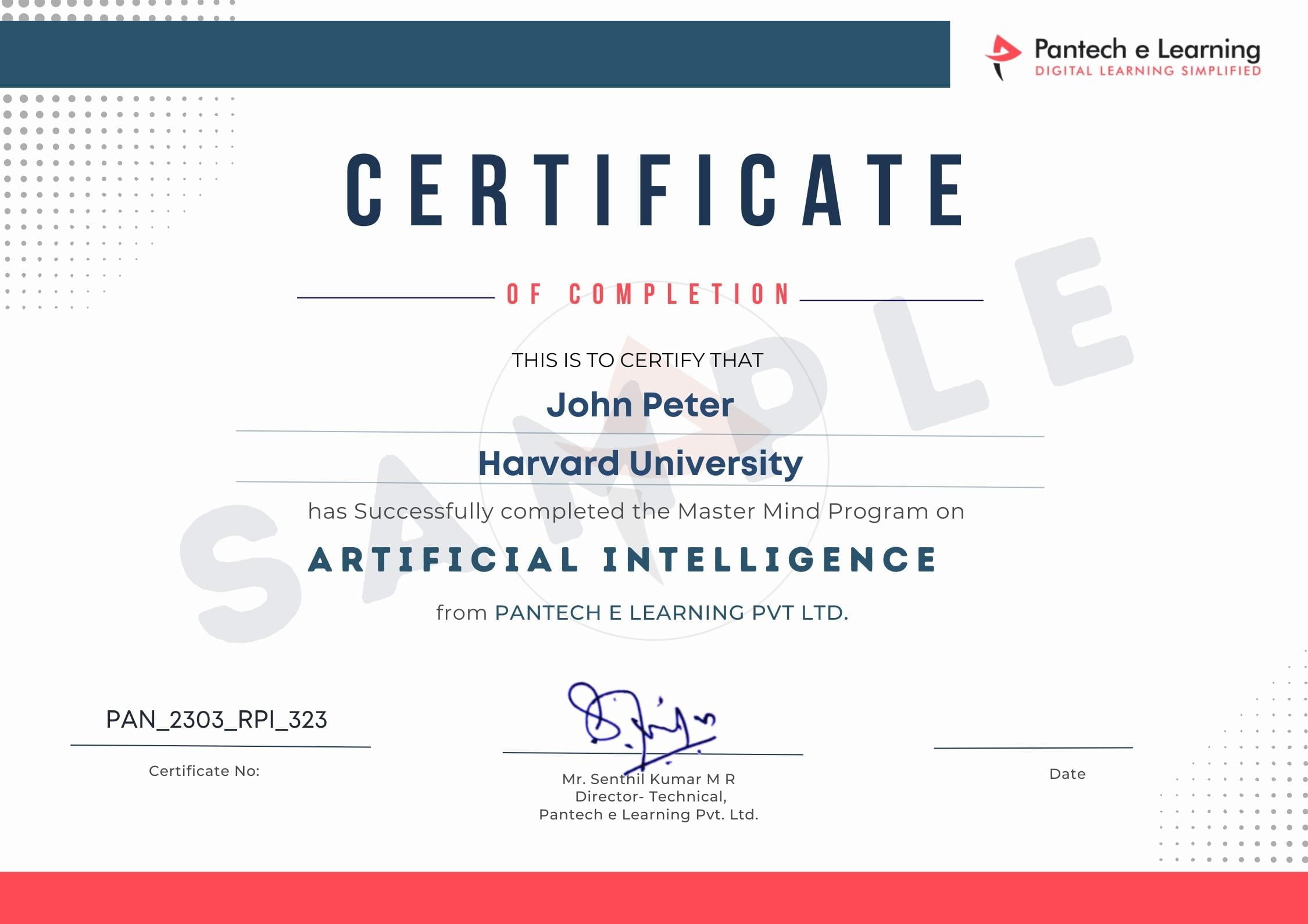
Step 4 Certification
✓ Get Certified
✓ E Certificate of Internship
✓ Project Completion Certificate
✓ Share on social media
✓ Get Job Notifications
✓ Exclusive Videos with detailed explanation
✓ Assignments & Projects
✓ Flexible Time
✓ New Lectures on the current trend
✓ Participation Certificate
✓ 4 LIVE intractive Mastermind Sessions
✓ 90 Days from the date of payment
✓ 4+ Capstone Projects & Codes
✓ 1 Month Internship Certificate
✓ Exclusive Videos with detailed explanations
✓ Assignments & Projects
✓ Flexible Time
✓ New Lectures on the current trend
✓ Participation Certificate
✓ 4 LIVE interactive Mastermind Sessions
✓ 180 Days from the date of payment
✓ 12+ Capstone Projects & Codes
✓ 2 Month Internship Certificate
The PCB Design Internship Program is a Virtual Internship Program. This is a mix of Recorded Sessions + LIVE Weekly Mastermind Sessions and Project Development.
Anyone with an interest in PCB Design can take this Internship. Students, professionals, and hobbyists with a zeal for the electrical /electronics domain.
The curriculum of this program is designed to provide technical knowledge from scratch. Hence No prior knowledge or coding experience is required. Participants are provided with KT from the basics
Once registered for this program, you shall get access credentials to our LMS Portal. You can make use of the same and access the program. You can learn and practice from desktop or from mobile using our Dedicated Mobile App.
The Internship Program comes in two Durations. One Month and Two Month Certification. However, you will have access to the records and the presentations for a period of 90 Days from the date of Registration.
Yes, you will be provided with Dual Certifications. Certificate of Internship Completion and Certificate of Mastermind Participation. Certificates will be available to download on the same LMS Portal.
Yes, this is a Recognised and Certified Internship. You can have a valuable addition to your resume. Pantech is a Technical Equipment cum training company which is in this Industry for 18+ Years of Experience
For recruitment within Pantech, we give preference to those who have completed an Internship with us. Job Notifications pertaining to PCB Design are provided. You can have a valuable addition to your resume.


